Pll Noise Floor

Phase Locked Loop Pll Fundamentals Analog Devices

Phase Locked Loops For High Frequency Receivers And Transmitters Part 2 Analog Devices

Pll Synthesizers Analog Devices

Low Cost Pll With Integrated Vco Enables Compact Lo Solutions Analog Devices

How To Design And Debug A Phase Locked Loop Pll Circuit Analog Devices

Designing High Performance Phase Locked Loops With High Voltage Vcos Analog Devices

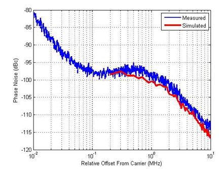
Loop of the pll.
Pll noise floor. That was the sweep that took the longest 120 seconds on the hp8568b. Pll normalized phase noise 9 log frequency bw everything except vco vco g a i n d b 0 20 log n pll flat noise fom pn1hz pll noise floor normalized to1 hz n counter added noise 20 log n pll flicker noise pn10khz usually dominates at offset below 1 khz pll 1 f normalized to 1 ghz output and 10khz offset. Phase noise pll phase noise ref 20 log f pll f ref dbc hz. Figure of merit in a pll is the normalized phase noise floor of the phase detector.
The unit of measurement is dbc hz. This is generally synthesizer divider noise and phase detector noise. For instance if dithering is disabled typically the noise floor does not degrade at all and just spurs are added. L floor l 1hz 20log 10 n 10log 10 f c 2 in band phase noise floor.
The loop continued until the noise floor was at or below the maximum permissible discrete spur level. For fractional mode it depends on the fraction. Noise is flat typically passed 15 or 20 mhz offset frequency and is called the noise floor of the source. The in band phase noise floor from the pll ic can be then determined by.
Adisimpll v3 3 and higher now models both. For newer pll devices we are actively improving our 1 f performance through design an example of this is the improvement in 1 f noise seen going from the adf4350 to the adf4351 pn1 f goes from 111dbc hz to 116dbc hz. The phase detector noise floor is estimated by measuring the in band noise at the vco output and subtracting 20 log n where n is the n divider value and 10 log fpfd where fpfd is the phase detector frequency. Phase noise floor measurement the basic phase lock loop configuration we will be consider ing is shown in figure 3.
Finally the phase noise typically scales with the output frequency so that half the frequency will improve the phase noise by 6 db. However the time savings came from the fact that if a violation was detected at a wider rbw. For wide loop bandwidths 50khz the normalized noise floor becomes important.

Max2880 250mhz To 12 4ghz High Performance Fractional Integer N Pll Maxim Integers Circuit Diagram Modulators

Phase Noise Simulation Phase Noise Simulation Keysight Knowledge Center

Pll Concepts Pll Concepts Keysight Knowledge Center

Figure 4 From Pll Phase Noise Modeling By Pc Semantic Scholar

Car Lock System Using Arduino And Gsm Arduino Arduino Board Circuit Diagram

Figure 7 From Pll Phase Noise Modeling By Pc Semantic Scholar

Zl2pd Tiny85 Si5351 Vfo Bfo Ham Radio Radio

Signal Chain Basics 71 How Supply Noise Impacts Clocking Devices

Fractional N Pll With Integrated 6ghz Vco Delivers Fractional N Benefits Without Complexity Or Performance Downsides Analog Devices

Circuit Diagram Of Fm Demodulation Circuit Design Circuit Circuit Diagram

Unlock And Load Characterizing Today S Plls
Silicon Accurate Fractional N Pll Design

Download Scientific Diagram 9 Volt Dual Power Supply Circuit Using Icl7660 Voltage Converter From Publi Power Supply Circuit Voltage Converter Power Supply

